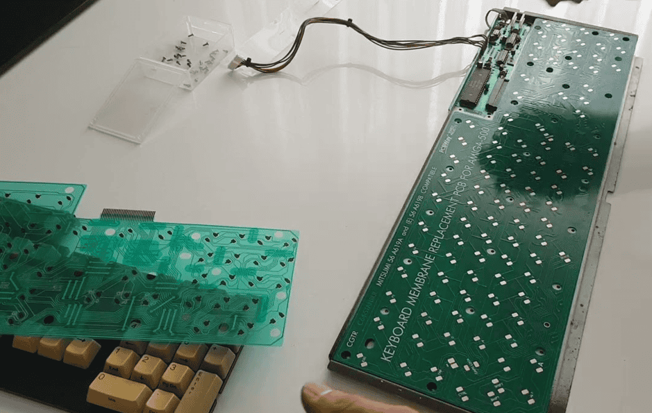
The design of printed circuit boards (PCBs) is a crucial aspect in the manufacturing of keyboards. This process implies developing a proper arrangement of the layout, which consists of electrical connections and components that are required for the keyboard’s functioning. Being the leading manufacturer in India, Linepro manufactures customized keypads that are keen on meeting the features of a customer’s requirements. This blog will explain what PCB design is, its categories, and steps in the process as well as practices to ensure a clear return path.
What is Printed Circuit Board (PCB) Design?
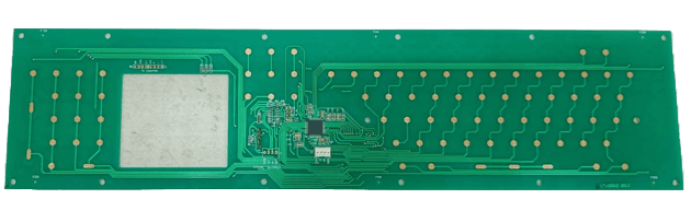
PCB design can be described as an activity of defining the layout of the circuit board that supports electronic components by using conductive tracks, copper pads, and other features and anodized on a non-conductive substrate. This design is the core when it comes to developing efficient and functional electronic devices, including keyboards.
Types of Printed Circuit Boards (PCBs)
Single-Sided PCBs: These have one layer of conductive material and these are the easiest categories of PCBs in the market.
Double-Sided PCBs: These have conductive material on both sides of the board and thus can support more circuits than the usual ones.
Multilayer PCBs: These are made of multiple layers of conductive material, and once again even more complex and versatile.
Flexible PCBs: These are designed to bend and fold, mostly for use where material flexing is required.
Rigid-Flex PCBs: These incorporate both the rigid board technology and the flexible board technology, and due to this; they have varying designs and uses.
The Process of Printed Circuit Board Designing
Step 1: Schematic Design
The first step is the creation of a schematic diagram, which shows the path or routes of the electrical connections. Concerning the present lens, this schematic can be considered as the template for the PCB layout.
Step 2: Component Placement
Next, components are placed to this layout of
the printed circuit boards. This is true because proper placement affects the overall performance as well as the usability of the equipment. Issues like signal interconnectivity, heat dissipation, and manufacturability are taken into account.
Step 3: Routing
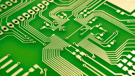
Routing involves connecting the placed components with copper traces. This step requires careful planning to avoid interference and ensure reliable signal transmission. Advanced software tools are often used to automate this process and optimize the design.
Step 4: Layer Stack-Up
In power PCBs, a layer stack-up is given and in the case of multilayer PCBs there is also a layer stack-up. Here it is necessary to define the position of conductive and non-conductive layers, which contributes to the control of signal propagation and electrical noise.
Step 5: Design Rule Check (DRC)
Post routing a DRC is carried out to check its compliance to the PCB layout manufacturing limits and electrical requirements. It is useful in the preparation step since it highlights areas of concern that need rectification before engaging in production.
How to Make a Printed Circuit Board
Step 1: Material Selection
Choosing the right substrate material is crucial. Common materials include FR4 for rigid boards and polyimide for flexible printed circuit boards.
Step 2: Printing the Design
The PCB design is printed onto the substrate using various methods such as silk screen printing, photographic methods, or advanced digital printing techniques.
Step 3: Etching
The unwanted copper is removed through an etching process, leaving behind the desired circuit pattern. This is typically done using chemical solutions.
Step 4: Drilling
Holes are drilled into the PCB to accommodate components and vias. Precision drilling is essential to ensure proper alignment and connectivity.
Step 5: Plating
The drilled holes are plated with conductive material to create electrical connections between different layers of the PCB.
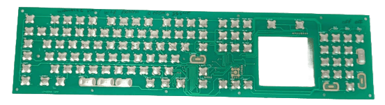
Step 6: Solder Mask Application
A solder mask is applied to protect the copper traces and prevent solder bridges during component assembly. This step enhances the durability and reliability of the PCB.
Step 7: Component Assembly
Finally, components are assembled onto the PCB using techniques such as surface-mount technology (SMT) or through-hole technology. This step involves precise placement and soldering of components.
Ensuring a Clear Return Path
A clear return path is crucial when handling signals since it will increase signal quality, and minimize the cases of electromagnetic interferences. This can be managed by paying a lot of attention to the layout to help make sure that the return current paths are as short as possible. Also, proper layout such as using ground planes and proper placement of the decoupling capacitors plays a very important role in the reduction of the noise that affects the microcontroller and increases its stability.
Conclusion
PCB design for the keyboard is a critical procedure that, though quite intricate, is of extreme importance in the development of an efficient and long-lasting product. Every aspect, right from choosing the right material to guaranteeing the right path for the transmitted signals has to be carefully thought out. Linepro is India’s leading printed circuit board manufacturer and providing customized keypads as per the client’s requirement.
For all your PCB board design and manufacturing needs, Linepro’s services are what you need for your custom needs. Please contact us now to find out how we could help you with your PCB and assembly requirements and surge ahead Visit us at www. lineproindia.com to know more
