The process of PCB designing includes different phases, and each stage comes with specific processes and checklists. For a successful PCB design, it is crucial to follow the steps and go through the checklist each time you reach a milestone. The first step in PCB design imparts foundation to overall PCB as we very well know the importance of PCBs in every walk of our lives. This article will go through the first step involved in designing PCBs using Altium Designer.
Step 1: PCB design schematic creation
The schematic drawing illustrates the components of a system by using graphic and abstract symbols. In this stage, the diagram is loaded into the tool for schematics (Altium, Allegro, etc.). A schematic lists the components that make up the design and how they are linked. Suppose the design employs the hierarchical model, where many functional schematics are interconnected. In that case, the schematic defines the connections between the component groups within different schematics—an example of a schematic diagram as follows:
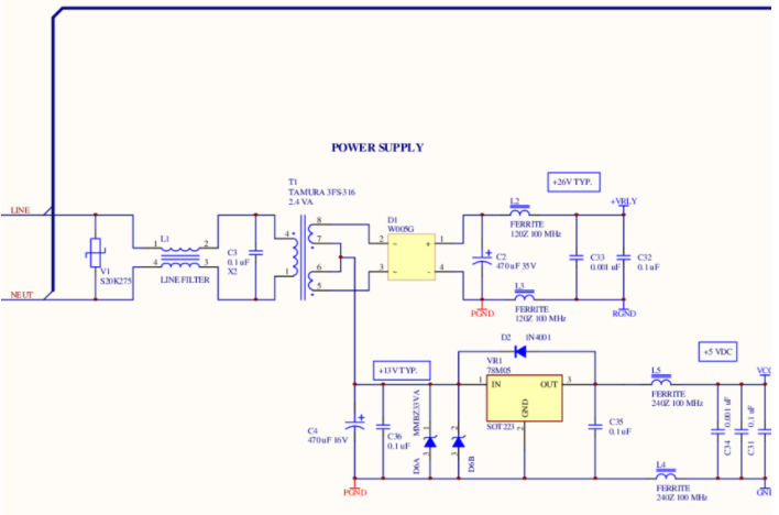
PCB design schematic diagram
It is the process of creating a conceptual representation of an electronic circuit. When you create an electronic schematic, you’re connecting elements (components) into a distinctive way making your unique electronic product.
Here are the steps required for PCB schematic creation with Altium Designer:
PCB design Schematic generation of symbols
Altium Designer’s symbol generation tool can be used by selecting the Tools and Symbol Wizard option in the menu. Creating symbols involves drawing the parts’ body, including Pin numbers and pins, and defining the reference designators and then assigning a footprint.
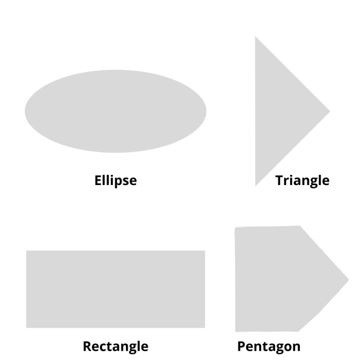
PCB design Schematic symbol placement
The construction of the symbol body is done by putting graphic designs in the workspace of the schematic library editor. Altium Designer includes a variety of closed symbol shapes such as pentagon, rectangle, ellipse and triangle, as illustrated below.
Pin numbering
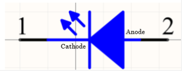
Pins determine the points of connection to the component used for inbound and outgoing signals. Pin numbering ensures the connections shown in the schematic are correctly connected by copper wiring on the PCB. The component pins provide components with their electrical characteristics and establish connections that direct signals into and out. A pin is used to represent every pin on the physical component.
Pins can be inserted into an electronic library document following some of these procedures:
1. Select Place->Pin on the main menu
2. Symbol Options dialogue will appear. The dialogue lets you define the height and width of the symbol and the pins’ length and a style for its pins concerning the ports on the source sheet. Then select OK.
Reference designators
Referral designators typically consist of the following: category, value, manufacturer, manufacturer’s part number, as well as supplier. It is suggested that each symbol in your circuit has its distinct designator so that each component is easily identified. For instance, every resistor must be named in a consistent sequence of R1, R2 or R3, etc.
The assignment of the footprint
Footprint provides an idea of the actual dimensions of the part. For instance, when we place a piece of equipment in the sand, it’ll leave its footprint there. This imprint represents its physical dimension. Specific components are available in standard packaging, and the footprints are simple to locate. In certain situations, it is necessary to create the footprint manually. Here are the steps to be followed to make a footprint using Altium Designer.
Make the pads
Key-in component height and area
Provide the silk-screen details
Save the footprint
Connecting the symbols
A PCB designer needs to illustrate how the components are connected. In the beginning, when two wires make up a junction and have the same electrical link, the intersection should be marked with the junction dot. This is the standard practice for every schematic design.
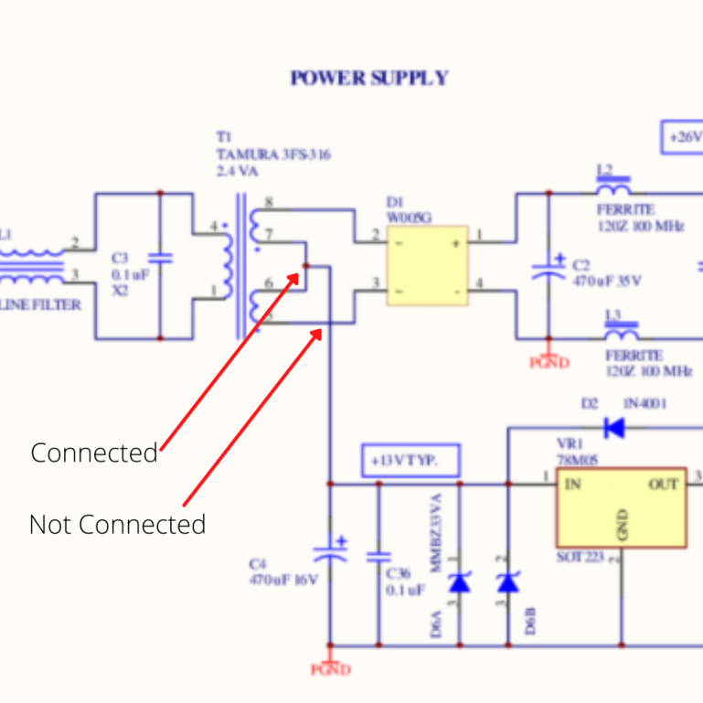
If you have two intersecting wires that aren’t electrically connected but over laps, you will not require dots.
The essential components on the circuit must be marked when connections are made to the component. This is a requirement for impedance tracks like 50 Ohms SE and 100 Ohms pairs of differentials. The power lines must be recognized and labeled.
Connect the footprints to the symbols
The components’ footprints are listed in the schematic diagram after you copy the schematic info onto the layout of your PCB.
Create the netlist
Netlist in any PCB designing software has information about the component’s name and the pad to which the component is connected. Netlist assigns numbers to the connections in order of serial. It also has a Netlist Manager dialogue used to manage and control the netlist on the board. Nets can be modified, added or deleted according to needs. Pins (or pads) of the elements inside the nets may also be edited.
Check your netlist
The Export Netlist option is utilized for exporting the netlist from the PCB to the current document. After the command is run, the netlist file with an extension of ‘.Net’ will be saved in the same folder as the circuit design document for the board is stored. A net by net check-in schematic must be completed (whether all nets are connected in an intended manner).
Generate BOM
A bill of material (BOM) is essentially an inventory of the materials needed to make the printed circuit board. Within Altium Designer, BOM can be made by selecting the option Report -> Bill of Materials from the PCB schematic.
It is advised to conduct an overall review following every step/sub-step to ensure a flawless design.
The first step of PCB design is very important step as it creates the outline of PCB along with details like schematic, symbols, pin allotment, Bill of Materials and netlist to name a few. PCB designing requires years of experience and to be updated about recent technological advancements helps in precise PCB design. At Linepro, we have a strong team of engineers and designers to cater every industry since last 29 years. Our Engineers and designers follow strict protocols and standard operating procedures to deliver customized PCB designs. Moreover, our experience of 29 years has helped us to gain relevant experience across any vertical of industry.