As opposed to the past technology, today’s gadgets continue to shrink in size. The majority of gadgets are now smaller and more efficient.
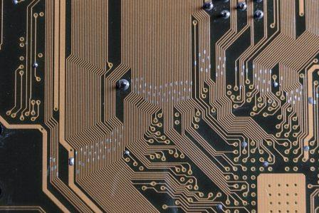
Problems with the issue of signal integrity in the PCBs or printed circuit boards pose an enormous challenge for designers.
Discontinuities, including irregular impedance or sharp bends, in addition to other things, can affect the integrity of signals in digital devices. In such events, a circuit becomes unstable, unreliable and in some instances even inoperable.
How can designers avoid this scenario? The answer is straight, by controlling impedance. This article will discuss strategies to prevent issues with signal integrity using impedance control.
1. Using Termination Resistors to avoid signal integrity issues
A terminating resistor can be crucial in order to prevent issues with signal integrity in PCB. The terminating resistors are signal quality components.
Designers use such resistors to soak the AC signals. This is to stop reflections onto the line. Incorrect impedance on transmission lines could cause issues with signal integrity.
Termination resistors create the required signal integrity. They improve speed and performance, while reducing the frequency of errors. When using termination resistors, designers are able to eliminate large amounts of noise. In this way, they will be able to improve the quality of signals during PCB design.
The primary purpose of the terminating resistor is to increase the signal integrity. However, engineers must pick the right one for their needs. They can choose from:
Parallel Termination,
AC Termination, RF Termination
Thevenin Termination
Series Termination
With a variety of designs, engineers should choose the most suitable termination techniques and resistors. They should select the ones that produce the desired signals in the circuit.
2. Maintenance of the same line impedance across a track length
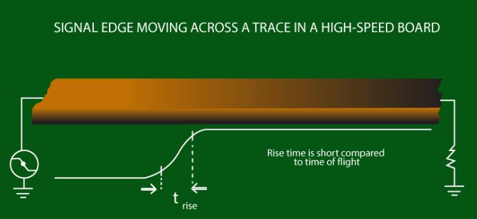
The capacitance and the inductance of an electrical trace circuit can have a significant impact on the electrical system. This is especially the case when the frequency is high. In addition, transmission lines in the course can become a problem. It is normal when a signal wavelength is not too far from trace length. This can lead to reflection and scattering of signal. All of these factors can negatively affect signal integrity in PCB.
To minimize the effects of transmission lines it is recommended to maintain the same line impedance. The line’s impedance requires support across the entire length of the track. This will make sure that you maintain the value of the impedance. By doing this, you can increase the signal integrity.
There are a variety of factors which influence impedance. One of the most significant is the distance between the trace and the ground. The other factors are line thickness and the dielectric constant of a printed circuit board. When ignored, all of these could lead to serious signal integrity issues.
3. Proper Grounding to reduce signal integrity problems
The control of Impedance indicates that circuit designers need to use the correct methods of grounding to ensure the signal is stable. If you use the right grounding methods, you can lessen the chance of damaging the signal. Grounding techniques can include:
1. Arranging the components to provide safe and quick return routes to the ground.
2. You can place the power and ground planes into the layers stack.
No matter what method you decide to employ, it is vital to be sure to use the proper techniques for grounding. By ensuring proper grounding, it is possible to avoid the occurrence of problems with signal integrity. In today’s highly-competitive industrial world, numerous items continuously interact with each other. This includes electrical plant, electronics, electric devices, electrical wiring and various other equipment for processing. These interactions can cause electromagnetic interference (EMI) and noise issues.
A proper grounding system can greatly assist in the reduction or elimination of electromagnetic interference and noise. So, designers can maintain the signal integrity in uniform manner.
4. Proper Routing
As with a good grounding system, the proper path is essential. If designers are trying to prevent signal integrity issues in PCB, it is vital to have a proper routing. When you think of electronic design, it is common to be able to hear the term “routing”. Wire routing, sometimes referred by the name- routing, is among the processes used when designing printed circuit boards.
In addition, routing all cables in the correct way is vital. This is especially essential to eliminate signal integrity issues.
Unfortunately, many circuit engineers tend to ignore this crucial step. For example, signal cables require routing away from electrical sources and all electrical devices.
The higher voltages are more likely to cause more electrical noise. Electrical noise can be an issue with signal integrity. For instance electric motors aren’t the most ideal choice since they are known to create a magnetic field. But, how far should you route your cables? The answer is dependent on factors like the magnitude of magnetic fields as well as the voltage. However, you must do the best you can to ensure you don’t have a noisy signal because of incorrect routing.
5. Use of Low-inductance Traces
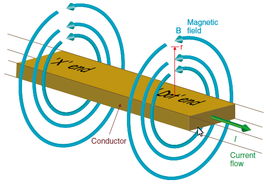
Inductors are coils that are able to store energy in form of magnetic field. They also resist changes that alter the course of current. Based on the place they will find their application, there are a variety of inductors. There exist high-frequency, low-frequency and power line inductors.
Inductors are able to resist changes in current and function like low-pass filters. They function as filters when they are in series with the power supply or the flow of signals. Inductors with high frequencies are susceptible to noise. Noise is not a good thing when it comes to maintaining signal integrity. If a frequency is higher, the impedance would be higher as well. The result is that noise is reduced and negatively impacting the signal integrity.
Designers who want to prevent signal integrity issues have a lot of advantages with low-inductance trace lines. Inductors with low frequencies aren’t susceptible to noise, as opposed to high-frequency.
6. Use of Broader line Spacing
Spacing is essential, regardless of whether it’s within your everyday life or in the field of circuitry. Imagine having a noisy neighbor. Do you not want to have a little more distance between yourself and your noisy neighbor? This is also true in the case of electronic circuits. Line spacing is vital in order to avoid issues with signal integrity in PCB.
Spacing is vital to avoid instances of flashover or tracking. Flashover and monitoring can happen between the electrical conductors. If you place your wires close to one another, monitoring and flashovers will happen. Flashovers and tracking will result in signal integrity issues. In order to avoid problems with signal integrity, you must have an effective separation between parallel traces with considerable space.
7. Applying Differential Routing Technique in Critical Parts
Differential routing is one method of design utilized in the creation of an efficient transmission system. The transmission system is able to carry the differential signals over an entire circuit. In the majority of cases, differential routing joins with another transmission device. Transmission systems may be connectors or cables.
There are numerous benefits that are associated from differential routing. At high speeds, electromagnetic interference and noise can begin to show up. This can weaken the signal. However, to avoid the risk of issues with integrity of the signal, it is crucial to utilize the differential routing. The use of differential routing is advantageous particularly in the most critical areas that comprise boards.
8. Use of Short Parallel run Lengths
Parallel length refers to the length or width that is between the edges of metal, or other elements. When it comes to issues related to circuits printed on boards similar lengths of runs are crucial. If two signals are running in close proximity, for a longer distance, you could face problems with the signal integrity in PCB. This is a problem you’d like to avoid at all costs.
The reason for this is that one signal could be the aggressor signal, with the other signal acting as the victim. To ensure that you don’t affect the signal integrity. it is recommended to choose short parallel run to avoid issues in signal integrity.
9. Using Short High-speed Signal Traces
As you might have guessed that high-speed printed circuit board design is often plagued by issues with Electro Magnetic Induction (EMI). EMI dangers originate from long traces that make up transmitting or receiving antennas. Longer trails are more likely to extend a considerable distance. Longer traces negatively impact the circuit’s sensitive components which can lead to problems with signal integrity in PCB.
Utilizing smaller high-speed bits that have the capability of taking direct routes can help reduce the dangers of EMI. The long and winding trails that are in your circuit could cause a lot of expense and cause issues with signal integrity. If you ensure that your trails aren’t too long, nobody will find your designs undesirable.
10. Shielding PCBs Sensitive Components
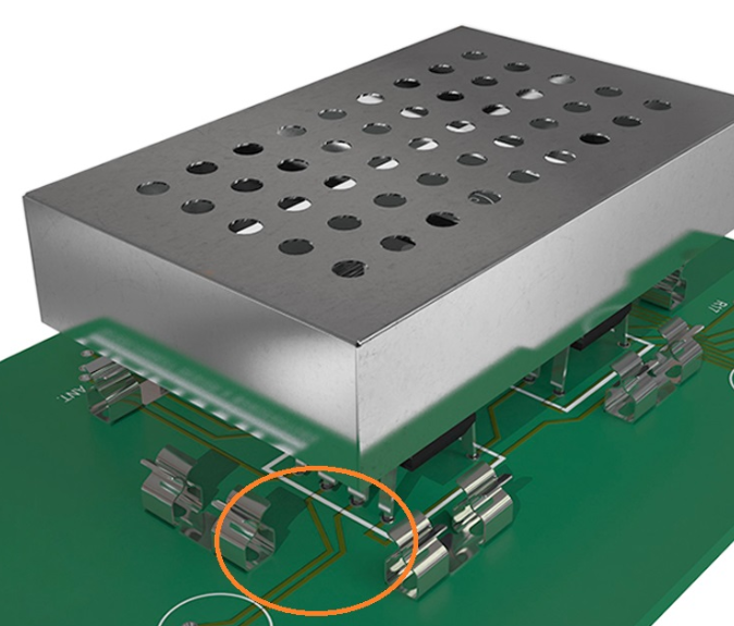
There are many sensitive components in a single PCB. PCBs consist of high precision resistors, computer cards, TTL chips and diodes. These components need shielding. Lack and poor shielding affects these parts permanently which ultimately causes issues with signal integrity. Shielding sensitive components cuts noise and improves signal integrity.
11. Signal Degradation due to cross-talk
A rapid current or voltage transition on the return path or signal line plane could cause it to couple with adjacent signal lines , creating unwanted signals known as crosstalk or switching noises on nearby signal lines. The coupling is caused by mutual capacitance and mutual inductance between the lines. The mutual capacitive and inductive coupling can be eliminated by increasing the distance between the trace. As a general rule the space should be three times trace length (3W). Also, faster rise time signals can cause crosstalk as well as switching noise.
Noise from switching and crosstalk can be reduced through:
Increasing the separation between signal traces
The signal return paths should be as wide as possible as well as uniform, similar to uniform planes and avoiding split return paths.
Utilizing a lower dielectric constant PCB material.
Using differential signaling and tightly coupled differential pairs, which are more immune to crosstalk.
Conclusion
In the end, you’ll need a reputable company that can design your circuits. The importance of a reliable PCB ensures service free record of machinery and hence prevents breakdowns and overhauls. If you want high-quality circuits with no issues with integrity, you’ll need to locate an industry-leading manufacturer. It will be helpful to have a supplier who communicates with you. They should also give you additional ideas.
Linepro has set the standard for others in the market in the designing of PCBs. If you want circuits that have no issues with signal integrity get in touch with us. We’ve been working on this for about 30 years and are able to get it perfect every time. Are you interested in more information regarding impedance control? What are the best ways to take control of the signal integrity of your printed circuit board? Please contact us for assistance.